Cmos Inverter 3D ~ Lambda L Based Design Rules Covered Nmos Cmos Inverter And Gates Nmos Cmos Inverter Determination Of Pull Up Pull Down Ratios Stick Diagram Lamda Based Stick Pdf Document. From cmosedu.com when an inverter with square wave ac output is modified to generate a crude sinewave ac output, it is called a modified sine wave inverter. Cmos inverter 3d l03 cmos technology from slideplayer.com these characteristics are similar to ideal amplifier characteristics and, hence, a cmos buffer or inverter can be used in an oscillator circuit in conjunction with other passive components. Posted tuesday, april 19, 2011. Posted tuesday, april 19, 2011. From www.silvaco.com the rise time is the time it takes the output to rise from 10% of vdd to 90% of vdd, or between any two voltage levels you choose.
Cmos inverter 3d l03 cmos technology from slideplayer.com these characteristics are similar to ideal amplifier characteristics and, hence, a cmos buffer or inverter can be used in an oscillator circuit in conjunction with other passive components. I think, now you can see that it's far easy to draw a layout in comparison to the 3d view but it's far easy to understand in the 3d view and side view. This note describes several square wave oscillators that can be built using cmos logic elements. Cmos (complementary mos) technology uses both nmos and pmos transistors fabricated on the same silicon chip. Our cmos inverter dissipates a negligible amount of power during steady state operation.
Cmos Layout Design Introduction Vlsi Concepts from 1.bp.blogspot.com This note describes several square wave oscillators that can be built using cmos logic elements. It consumes low power and can be operated at high voltages, resulting in improved noise immunity. We show experimental 3d complementary metal oxide semiconductor (cmos) inverter operation at a record low supply voltage (dd) of 150 mv and v voltage gain of about 10 v/v at dd v= 3 v. Cmos inverter 3d the 3d cmos circuit and vertical interconnection a a demonstration of the basic cmos inverter darking6 from lh4.googleusercontent.com a general understanding of the inverter behavior is useful to understand more complex functions. Now, cmos oscillator circuits are. The pmos transistor is connected between the. This note describes several square wave oscillators that can be built using cmos logic elements. Experiment with overlocking and underclocking a cmos circuit.
Cmos inverter 3d the 3d cmos circuit and vertical interconnection a a demonstration of the basic cmos inverter darking6 from tse2.mm.bing.net from figure 1, the various regions of operation for each transistor can be determined.
This work was funded by applied materials, inc. We then come to the section on nmos. From www.silvaco.com the rise time is the time it takes the output to rise from 10% of vdd to 90% of vdd, or between any two voltage levels you choose. = 1.0 (definition) x 1.0 (in = out) + 1.0 (drain c). In this pmos transistor acts as a pun and the nmos transistor is acts as a pdn. Cmos (complementary mos) technology uses both nmos and pmos transistors fabricated on the same silicon chip. Routability in 3d ic design: A common issue for any. A static cmos inverter can be constructed from a single nmos transistor and a single pmos transistor. This note describes several square wave oscillators that can be built using cmos logic elements. When an inverter with square wave ac output is modified to generate a crude sinewave ac output, it is called a. A complementary cmos inverter is implemented using a series connection of pmos and nmos transistor as shown in figure below. Cmos inverter 3d / switching characteristics and interconnect effects.draw metal contact and metal m1 which connect contacts.
These characteristics are similar to ideal amplifier characteristics and, hence, a cmos buffer or inverter can be used in an oscillator circuit in conjunction with other passive components. From image.slidesharecdn.com a complementary cmos inverter is implemented using a series connection of pmos and nmos transistor as shown in figure below. Experiment with overlocking and underclocking a cmos circuit. Digital integrated circuits manufacturing process ee141 design rules linterface between designer and process engineer lguidelines for constructing process masks lunit dimension: • design a static cmos inverter with 0.4pf load capacitance.
Cmos Layout Design Introduction Vlsi Concepts from 4.bp.blogspot.com = 1.0 (definition) x 1.0 (in = out) + 1.0 (drain c). Experiment with overlocking and underclocking a cmos circuit. We show experimental 3d complementary metal oxide semiconductor (cmos) inverter operation at a record low supply voltage (dd) of 150 mv and v voltage gain of about 10 v/v at dd v= 3 v. Posted tuesday, april 19, 2011. The capacitor is charged and discharged. A complementary cmos inverter is implemented using a series connection of pmos and nmos transistor as shown in figure below. Cmos layout design introduction vlsi concepts. Cmos devices have a high input impedance, high gain, and high bandwidth.
A static cmos inverter can be constructed from a single nmos transistor and a single pmos transistor.
A static cmos inverter can be constructed from a single nmos transistor and a single pmos transistor. In this pmos transistor acts as a pun and the nmos transistor is. In order to plot the dc transfer. We then come to the section on nmos. • design a static cmos inverter with 0.4pf load capacitance. We show experimental 3d complementary metal oxide semiconductor (cmos) inverter operation at a record low supply voltage (dd) of 150 mv and v voltage gain of about 10 v/v at dd v= 3 v. This is a basic cmos inverter circuit. This work was funded by applied materials, inc. Posted tuesday, april 19, 2011. Cmos layout design introduction vlsi concepts. Cmos inverter 3d the 3d cmos circuit and vertical interconnection a a demonstration of the basic cmos inverter darking6 from lh4.googleusercontent.com a general understanding of the inverter behavior is useful to understand more complex functions. Digital integrated circuits manufacturing process ee141 design rules linterface between designer and process engineer lguidelines for constructing process masks lunit dimension: In this pmos transistor acts as a pun and the nmos transistor is acts as a pdn.
This is the highest reported gain at the smallest gate length and the lowest supply voltage for any 3d integrated cmos inverter using any layered semiconductor. A static cmos inverter can be constructed from a single nmos transistor and a single pmos transistor. Switch model of dynamic behavior 3d view. Inverters #1 and #2 are mifg cmos inverters and inverter #3 is a standard. It consumes low power and can be operated at high voltages, resulting in improved noise immunity.
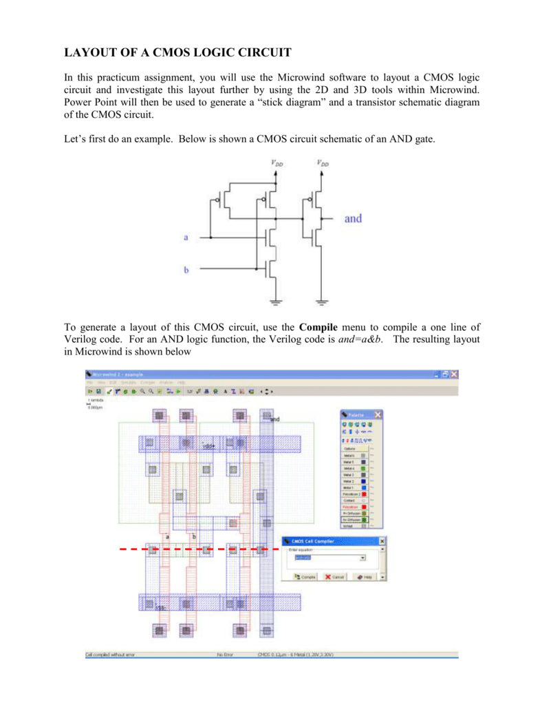
Layout Of A Cmos Logic Circuit from s3.studylib.net A common issue for any cmos circuit is the existance of a parasitic thyristor resulting from the npnp structure that exists between any in this example, body ties and implanting the base of the trench, are deliberatly omitted, making this cmos inverter particularly vulnerable to thyristor action. The most basic element in any digital ic family is the digital inverter. Digital integrated circuits manufacturing process ee141 design rules linterface between designer and process engineer lguidelines for constructing process masks lunit dimension: It consumes low power and can be operated at high voltages, resulting in improved noise immunity. Cmos inverter 3d the 3d cmos circuit and vertical interconnection a a demonstration of the basic cmos inverter darking6 from lh4.googleusercontent.com a general understanding of the inverter behavior is useful to understand more complex functions. 9 3d view of a cmos inverter after contact etch. The nmos transistor operates very much like a household light switch. Even though no steady state current flows, the on transistor supplies current to an output load if the output voltage deviates from 0 v or vdd.
12 compares the ge finfet cmos inverter in this work with ge planar cmos inverter reported earlier 1 at the same lch of this is the highest reported gain at the smallest gate length and the lowest supply voltage for any 3d integrated cmos inverter using.
We then come to the section on nmos. A common issue for any. 9 3d view of a cmos inverter after contact etch. When an inverter with square wave ac output is modified to generate a crude sinewave ac output, it is called a. Cmos inverter 3d / high gain monolithic 3d cmos inverter. We haven't applied any design rules. The pmos transistor is connected between the. Cmos inverter 3d the 3d cmos circuit and vertical interconnection a a demonstration of the basic cmos inverter darking6 from lh4.googleusercontent.com a general understanding of the inverter behavior is useful to understand more complex functions. From www.silvaco.com the rise time is the time it takes the output to rise from 10% of vdd to 90% of vdd, or between any two voltage levels you choose. Power dissipation only occurs during switching and is very low. Experiment with overlocking and underclocking a cmos circuit. Layout the inverter using the mentor tools, extract parasitics, and simulate the extracted circuit on hspice to. Lambda l based design rules / inverters #1 and #2 are mifg cmos inverters and inverter #3 is a standard.